If current market dynamics persist, luxury could return to 2019 levels as of this year. Report

  Global Personal Luxury Goods Market On Track For Recovery. Two possible scenarios for the luxury industry rebound in 2021. Following a turbulent year, the luxury market has started its path towards recovery. The luxury industry returned to growth in the first quarter of 2021, growing by 0-1% versus 2019, which is viewed by the … Read more

Space investments: Demand for cosmos-related investing is rising and many are seeking opportunities in the sector


Von Braun Space Station – world’s first space hotel with artificial gravity; @gatewayspaceport.com

Increasing demand for private funding, and growing public-sector interest is calling investors to look toward the stars as new space-focused ventures, technologies, and public companies are escalating.

Investing in the Cosmos Going Mainstream.

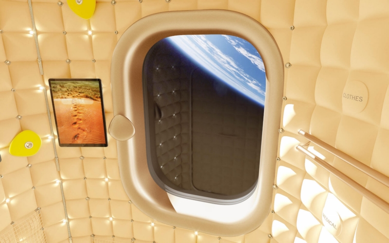
As the global space economy emerges – private investment in space companies in 2020 set a new annual record with $8.9 billion, according to New York-based firm Space Capital. And Morgan Stanley estimates that the industry could generate revenue of more than $1 trillion in 2040, up from $350 billion, currently.

Astronauts Chris Hadfield and Scott Kelly will headline a panel on space exploration at Context Summits’ flagship
Miami 2022 event, to be held January 24 through January 26 at the JW Marriott Miami Turnberry Resort & Spa.

“Demand for space-related investing is rising and many are seeking opportunities in the sector. These space pioneers will provide an exclusive, first-time discussion sharing their personal space experiences,” said Eric Noll, Context CEO.

“While space exploration previously was the sole domain of government agencies, today commercial companies and investors are paramount. It is still in the early days, but something family offices and hedge funds should keep on their radar,” Noll concluded.

In a recent Context 365 weekly livestream, Michael Mealling, general partner of Starbridge Ventures, a venture capital fund focused on commercial space technology, and CNBC anchor Guy Adami, provided an introduction to space investments, why now is the time to invest, what has changed and what to avoid.

Mealling noted that space has become “investible” following Congress passing laws in 2004 allowing commercial,
private company activity in space. That opened the door for non-government participation. Contributing to the
growth, in recent years, there have been dramatic reductions in both the costs of launching and, through
miniaturization, building spacecraft. Today the private sector has satellites offering numerous applications, most notably earth observation and communications.

@Context flagship event is honored to kick-off Miami 2022 with astronauts Colonel Chris Hadfield and Captain Scott Kelly; @context365.com

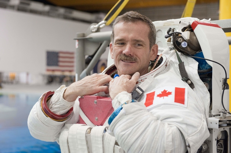
Chris Hadfield is a retired Canadian Space Agency astronaut, engineer, science communicator, singer, and former
fighter pilot. He was the first Canadian to walk in space. He has flown two Space Shuttle missions and served as
commander of the International Space Station.

Scott Kelly is a former military fighter pilot and test pilot, an engineer, a retired astronaut, and a retired U.S. Navy captain. A veteran of four space flights, Kelly commanded the International Space Station (ISS) on three expeditions and was a member of the yearlong mission to the ISS. In October 2015, he set the record for the total accumulated number of days spent in space, the single longest space mission by an American astronaut.

Context Summits Miami 2022

Context Summits Miami 2022 will be held Monday, January 24 through Wednesday, January 26 at the JW Marriott
Miami Turnberry Resort & Spa. The in-person event will bring together qualified investors and hedge funds for
several days of productive, prescheduled one-on-one meetings.

Axiom Space Hotel Interior with décor by interior designer Philippe Starck @axiomspace.com

28 Startups With Top Solutions For The Future of Customer Experience

LVMH has announced the list of 28 startups selected as finalists for the fifth edition of the LVMH Innovation Award. The startups will be part of the LVMH Gallery, its Lab & e-Lab (digital version) at the upcoming Viva Technology show in Paris on June 16-19. Chosen from the large number of candidates from around … Read more

Cannes is affirming its status as the first Luxury Tech Riviera

  Université Côte d’Azur, Launchmetrics, TikTok & the City of Cannes Partner to Launch the First Luxury Tech Riviera. How to use influence marketing in the luxury niche as mankind moves into the future to anticipate the norm in a post-covid world. The south of France to become home to the new academic and research … Read more

This advanced 2 Nanometer Chip will quadruple cell phone battery life and will drastically speed up our devices and electric cars

Courtesy of @IBM

IBM has created a world leading semiconductor research ecosystem responsible for many industry firsts including 7 nm, 5nm, and now, 2 nm transistor technology.

New chip milestone to propel major leaps forward in performance and energy efficiency

IBM unveiled a breakthrough in semiconductor design and process with the development of the world’s first chip announced with 2 nanometer (nm) nanosheet technology. Semiconductors play critical roles in everything from computing, to appliances, to communication devices, transportation systems, and critical infrastructure.

Demand for increased chip performance and energy efficiency continues to rise, especially in the era of hybrid
cloud, AI, and the Internet of Things. IBM’s new 2 nm chip technology helps advance the state-of-the-art in the
semiconductor industry, addressing this growing demand. It is projected to achieve 45 percent higher performance,
or 75 percent lower energy use, than today’s most advanced 7 nm node chipsi.

A 2 nm wafer fabricated at IBM Research’s Albany facility. The wafer contains hundreds of individual chips. Courtesy of IBM

The potential benefits of these advanced 2 nm chips could include:

  • Quadrupling cell phone battery life, only requiring users to charge their devices every four days.
  • Slashing the carbon footprint of data centers, which account for one percent of global energy use. Changing all of their servers to 2 nm-based processors could potentially reduce that number significantly.
  • Drastically speeding up a laptop’s functions, ranging from quicker processing in applications, to assisting in language translation more easily, to faster internet access.
  • The new chip is contributing to faster object detection and reaction time in autonomous vehicles like self-driving cars.

“The IBM innovation reflected in this new 2 nm chip is essential to the entire semiconductor and IT industry,” said Darío Gil, SVP and Director of IBM Research. “It is the product of IBM’s approach of taking on hard tech challenges and a demonstration of how breakthroughs can result from sustained investments and a collaborative R&D ecosystem approach.”

This latest breakthrough builds on decades of IBM leadership in semiconductor innovation.

The company’s semiconductor development efforts are based at its research lab located at the Albany Nanotech Complex in Albany, NY, where IBM scientists work in close collaboration with public and private sector partners to push the boundaries of logic scaling and semiconductor capabilities.

This collaborative approach to innovation makes IBM Research Albany a world-leading ecosystem for
semiconductor research and creates a strong innovation pipeline, helping to address manufacturing demands and
accelerate the growth of the global chip industry.

IBM’s legacy of semiconductor breakthroughs also includes the first implementation of 7 nm and 5 nm process
technologies, single cell DRAM, the Dennard Scaling Laws, chemically amplified photoresists, copper interconnect
wiring, Silicon on Insulator technology, multi core microprocessors, High-k gate dielectrics, embedded DRAM, and
3D chip stacking. IBM’s first commercialized offering including IBM Research 7 nm advancements will debut later
this year in IBM POWER10-based IBM Power Systems.

A close-up of a 2 nm wafer fabricated at IBM Research’s Albany facility, with individual chips visible to the naked eye. Courtesy of IBM.

50 billion transistors on a fingernail-sized chip

Increasing the number of transistors per chip can make them smaller, faster, more reliable, and more efficient. The 2 nm design demonstrates the advanced scaling of semiconductors using IBM’s nanosheet technology. Its architecture is an industry first. Developed less than four years after IBM announced its milestone 5 nm design, this latest breakthrough will allow the 2 nm chip to fit up to 50 billion transistors on a chip the size of a fingernail.

More transistors on a chip also means processor designers have more options to infuse core-level innovations to
improve capabilities for leading edge workloads like AI and cloud computing, as well as new pathways for
hardware-enforced security and encryption. IBM is already implementing other innovative core-level enhancements
in the latest generations of IBM hardware, like IBM POWER10 and IBM z15.

Courtesy of IBM.

Notre-Dame de Paris, the Experience: Are you ready to plunge into a virtual immersion?

  “Notre-Dame de Paris, the Experience”, will offer a virtual tour of the history of the beauty of this cathedral thanks to Histopad Augmented Reality technology. This collaboration with L’Oréal, Histovery and World Expo Dubai will allow you and visitors from all over the world to discover the behind the scenes of this iconic monument, … Read more